Initializing lattice

Quantum-Grade Materials & Components

Every atom, precisely placed for your science

Your Research, Powered by Our Epitaxy. Stop troubleshooting deposition and start publishing results. We leverage 20 years of MBE expertise to grow your complex heterostructures atom by atom, exactly to spec.

Now accepting growth requests

Let's meet face to face

We're heading to the March Meeting and we'd love to sit down with you. Reach out to schedule a conversation — we have something exciting to share.

0

Years of MBE expertise

Å

Atomic-layer precision

III-V

Compound semiconductors

Your ideas deserve flawless materials

Your materials should be the foundation of your science, not the limit. We engineer the building blocks for topological states, quantum devices, and photonic systems so you can focus on the next breakthrough.

No MBE? No problem

  • World-class epitaxial growth without owning a system
  • We become your dedicated growth facility

Atom-by-atom control

  • Monolayer-level precision across every interface
  • Meticulous control of flux, temperature, and stoichiometry

Trusted by researchers

  • Reproducible, characterized, and fully documented
  • Every wafer ships with growth logs and citable data

Focus on physics

  • Spend time on measurements, not growth optimization
  • We handle materials science so you focus on discovery

Collaborative approach

  • Consultation on layer design and buffer strategies
  • Substrate selection optimized for your target application

Publication-grade quality

  • Engineered to meet top-tier journal standards
  • Our growth quality speaks through your results

The team behind the growth

Decades of combined expertise in molecular beam epitaxy, quantum materials, and device physics — from lab bench to publication.

Matt Shulman

Matt Shulman

Chief Executive Officer, Co-Founder
Prof. Javad Shabani

Prof. Javad Shabani

Chief Science Officer, Co-Founder
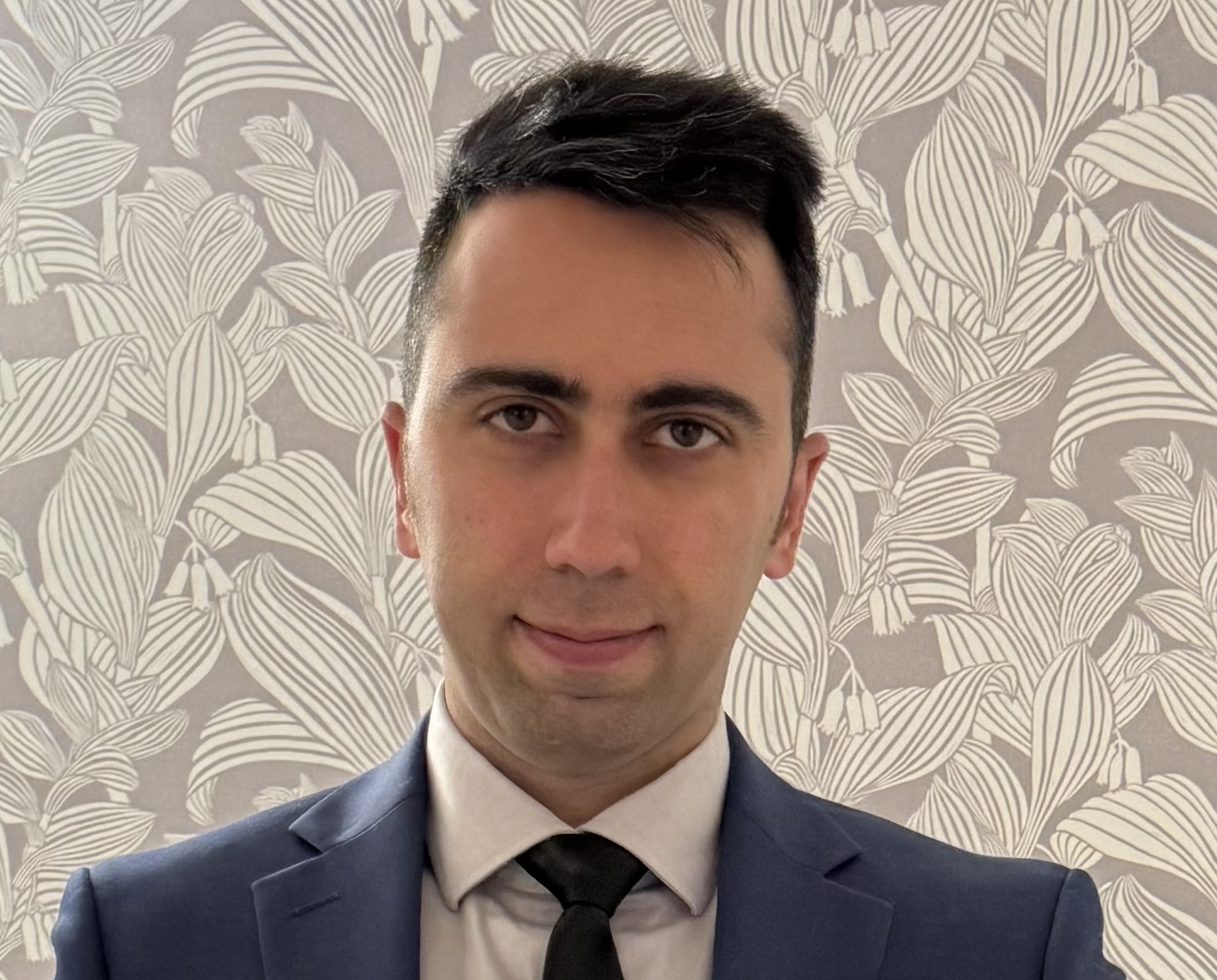
Dr. Mehdi Hatefipour

Dr. Mehdi Hatefipour

Head of Product
Dr. Maryam Barzegar

Dr. Maryam Barzegar

Head of Hardware Engineering
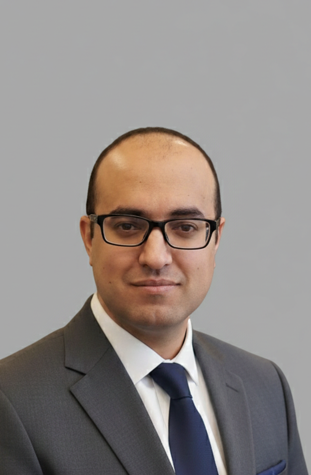
Dr. Ido Levy

Dr. Ido Levy

Head of Materials & Characterizations

Rooted in peer-reviewed research

Our materials and processes draw directly from published work in leading physics journals.

Precision-grown III-V heterostructures

Tailored epitaxial stacks for quantum transport, topological physics, superconductor-semiconductor hybrids, and optoelectronic devices

Indium Arsenide

InAs

High-mobility 2DEG systems, quantum wells, and nanowire-compatible thin films. Ideal for topological and mesoscopic physics

Quantum wells 2DEG High mobility

InAs / Epitaxial Al

InAs + epi-Al

Superconductor-semiconductor hybrid structures with pristine interfaces. Engineered for Majorana platforms, and gatemon qubits

Hybrid S-Sm Hard gap Majorana

GaAs / InGaAs

GaAs · InxGa1-xAs

Lattice-matched and strained heterostructures for HEMTs, photonics, and quantum dot systems with tunable bandgap engineering

HEMT Quantum dots Photonics

From concept to characterized wafer

A streamlined process designed to minimize your lead time and maximize material quality.

Step 01

Share your requirements

Tell us about your device structure, target properties, and application. We'll discuss feasibility and suggest optimizations.

Step 02

Growth design & planning

Our MBE specialists design the full layer stack — substrate prep, buffer layers, active regions, and capping — optimized for your target.

Step 03

MBE growth

Precision deposition in ultra-high vacuum. Real-time RHEED monitoring ensures crystalline perfection at every monolayer.

Step 04

Characterization & delivery

Structural and electronic characterization on every sample. Your wafer ships with growth logs and measurement data — ready for your lab.

Ready to accelerate your research?

Tell us about your project. Whether it's a single test wafer or a recurring growth campaign, we'll tailor a solution to your needs. Explore our materials to see what's possible.